
Chip fabs could process roughly 50% more wafers per hour on the most advanced lithography tools if ASML’s new extreme‑ultraviolet (EUV) light source reaches production as promised – but the company’s own timeline makes this a medium‑term capacity play, not a quick cure for today’s shortages.
ASML says it has a factory‑ready EUV light source that produces 1,000 watts — up from the ~600W baseline on current machines. The practical result, per ASML’s math, is faster exposure speeds: a machine that today runs roughly 220 wafers per hour could process about 330 wafers per hour with the higher‑power source. That’s a near 50% uplift in throughput per installed tool.
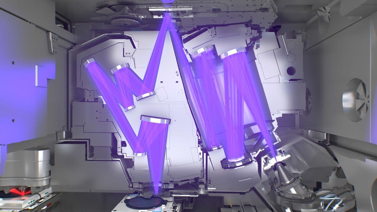
How does it work? The company’s existing EUV approach uses microscopic molten‑tin droplets that are zapped with high‑power lasers to produce the EUV photons. That “droplet + laser” engineering is fiendishly complicated — which is why ASML remains the only company shipping high‑volume EUV systems — but it’s also a lever you can turn to crank more light out of the same optical train.
Capacity is king. A 50% throughput increase per tool reduces the number of machines and clean‑room hours needed to hit a fab’s output target. For customers who are capacity‑constrained — think cloud datacenter GPU suppliers, mobile SoC makers, and console silicon — squeezing more wafers from the same capital base is a direct way to produce more chips without building new fabs overnight.
But there are two big caveats. First: ASML’s change increases the speed of processing wafers — it does not change the physics of defects or lithographic overlay that determine per‑wafer yield. In plain English: you can make more wafers faster, but not necessarily a higher percentage of good dies per wafer.
Second: ASML is targeting this as a commercial reality around 2030. That timeline matters. EUV’s transition from prototype to volume tool took years; getting customers to qualify, buy, and deploy new sources across a global installed base will also take time. So the supply relief arrives, but not immediately.
ASML is pitching a throughput headline — which is a real and useful metric — but the company’s statement sidesteps the rest of the production chain that actually delivers chips to consumers. Mask complexity, reticle throughput, back‑end assembly, test capacity, metrology bottlenecks, and the sheer logistics of installing and qualifying upgraded EUV sources at customers all dilute the simple “50% more chips” message.
And there’s the cost side: higher‑power sources may raise tool operating expenses, and fabs will weigh whether to retrofit existing scanners or wait for next‑generation units. The announcement doesn’t say how many current machines can be upgraded, what the upgrade downtime looks like, or how the new source affects maintenance intervals.
ASML’s claimed engineering is significant: brighter EUV is a straightforward way to multiply the output of a very expensive bottleneck. But this is a capacity story with qualifiers — timing, downstream bottlenecks, and operational tradeoffs all determine whether that 50% figure turns into 50% more chips on store shelves.
ASML says it has pushed EUV source power from 600W to 1,000W, which could raise throughput from ~220 to ~330 wafers/hour — about a 50% increase. That’s a real capacity multiplier for fabs, but it doesn’t change per‑wafer yields and ASML expects the improvement to be deployable around 2030. Watch ASML’s roadmap and major fabs’ retrofit plans — those will tell you if this is a late‑decade productivity win or just a headline today.
Get access to exclusive strategies, hidden tips, and pro-level insights that we don't share publicly.
Ultimate Gaming Strategy Guide + Weekly Pro Tips